
Printed Circuit Board Prototype
A printed circuit board (PCB) is a vital component of many electronic devices. PCBs are made from layers of conductive copper that connect the various electrical components to each other, as well as to the device power source. Prototypes of these boards are often created for use in the testing and design process to ensure that the final product will function as intended.
A prototyping process can save time and money in the long run by identifying flaws in the design before committing to full-scale production. In addition, it can reduce the risk of faulty or inefficient products by reducing manufacturing errors and eliminating costly rework. However, building a prototype is not an easy task and requires rigorous planning throughout the design, fabrication, assembly, and testing stages.
The first step in creating a printed circuit board prototype is to create a schematic diagram using a PCB design software, such as Altium Designer, Eagle, or KiCad. This will allow you to see how the components will fit on the board and determine the best location for each one, as well as lay out the traces that will connect them. A thorough schematic will also include a ground plane, which helps to reduce electrical noise and improve performance.
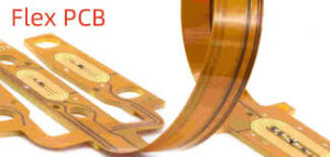
How is a Printed Circuit Board Prototype Made?
Next, the PCB must be prepared for the printing process. It is coated with a photosensitive material and exposed to UV light through a mask that represents the circuit pattern. This is known as “etching.” Once the desired pattern is revealed in the copper layer, it must be plated to protect and enhance conductivity. Then, holes must be drilled for the component leads. This is done with precision drilling equipment in a safe and well-ventilated area. The resulting PCB will be ready for assembly.
Depending on the complexity of the PCB, the fabrication process can take several days or weeks. This is because the prototype must be carefully sized to match the dimensions of the intended final product, and all the conductive pathways must be routed accordingly. During the manufacturing stage, careful consideration must be given to the choice of material, as this will affect the durability, reliability, and thermal properties of the finished product. Common PCB materials include FR4, a type of fiberglass, and polyimide. In some cases, a metal-core PCB may be required for specific applications that require enhanced thermal management.
Once the PCB is assembled, it must undergo extensive testing to ensure that the conductive pathways work as designed and that the components are connected properly. Any failures at this point will result in a redesign of the prototype or the final product.
If the prototype passes all the necessary tests, it is ready for production. This is a major step in the process, and should only be completed once all of the issues with the original prototype have been resolved. This may include a re-arrangement of the components, a change in the layout of the board, or a new design altogether.

