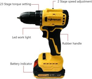
back drill work
In multilayered printed circuit boards, back drilling is a process that eliminates the via stub that remains in plated through holes (PTH). Unless removed, these stubs can cause reflection, scattering and delay problems during transmission of high-speed signals. This is a common issue in PCBs that require high signal integrity. This can result in distorted and corrupted data and poor performance. In order to avoid such issues, back drilling is used in high-speed and radio-frequency (RF) signal transmissions. This process removes the unused portions of PTH barrels, making them functional again.
The basic concept behind back drill is to create a new hole in the board that is bigger than the original via or pad hole to remove excess copper plating. The amount of oversize that is required is defined by the designer through a back drill design rule, and is displayed as a ring in the Layer Stack Manager. The colored ring is determined by which layer of the design the via or pad is on, with the inner circle representing the original via or pad hole size, and the outer ring showing the back drill hole size.
To set up a back drill, open the Layer Stack Manager and select Tools >> Features >> Back Drills. Then, click the button to add a new back drill definition. The back drill is only available if the feature is enabled. Once the back drill definition is added, you can select nets that need to be back drilled. For example, you might want to back drill all ethernet RX nets. After selecting the nets, click on the icon to add them to the back drill list.

How does back drill work?
Once you’ve added the nets, the next step is to select the back drill stub length and oversize parameters. The stub length is the remaining portion of the via left behind after the back drill is complete. The oversize parameter defines how much larger the back drill should be than the original via or pad hole size, and can be set in millimeters.
It’s important to choose the correct oversize for your project. Too little and you won’t achieve the desired level of signal integrity; too much and it will increase manufacturing costs. The best way to determine the right oversize for your project is by using a simulation, which will show you how much signal attenuation can be reduced.
The bottom line is that back drilling is necessary in any design where a high-speed signal needs to be transmitted between layers of the PCB. However, it is important to remember that other strategies can be used to reduce signal reflections in high-frequency applications.
For example, alternative stack-up arrangements can be used to prevent the need for back drilling in these cases. This allows designers to focus on ensuring that the signal can travel through all layers of the stack without any distortions. By using the right design techniques and PCB fabrication processes, you can make sure that your high-speed signals are transmitted without loss of integrity.

