
technology influence PCB fabrication assembly
Technology has dramatically transformed the way printed circuit boards (PCBs) are designed, fabricated, and assembled. As the demand for smaller, faster, and more complex electronic devices continues to grow, the role of advanced technology in PCB fabrication assembly has become even more critical. From automated machinery and precision manufacturing techniques to sophisticated software tools and materials innovations, technology plays a central role in enhancing the efficiency, speed, and quality of PCB fabrication assembly processes. In this article, we will explore how various technological advancements have influenced PCB fabrication assembly and how they continue to shape the future of electronics manufacturing.
One of the most significant technological influences on PCB fabrication assembly is the development of automation. Automation has revolutionized the assembly process by reducing manual labor and improving precision. Automated systems, such as pick-and-place machines, have made it possible to place components onto PCBs with incredible speed and accuracy. These machines can place thousands of components per hour, minimizing human error and ensuring consistent alignment and placement. Additionally, reflow ovens and wave soldering machines have automated the soldering process, further reducing the potential for mistakes and speeding up production. Automation not only increases the speed of assembly but also improves the overall quality of the final product by ensuring uniformity and reducing defects.
Another technological advancement that has significantly impacted PCB fabrication assembly is the use of advanced software tools. Electronic Design Automation (EDA) software allows engineers to design complex PCB layouts and schematics quickly and efficiently. These software tools, such as Altium Designer and Autodesk Eagle, enable designers to simulate electrical performance and optimize the layout before moving to the fabrication stage. By detecting potential issues early in the design process, such as signal interference or component placement conflicts, EDA tools help to avoid costly revisions and delays during assembly. Additionally, Bill of Materials (BOM) management software helps streamline the procurement and inventory process, ensuring that all components are readily available for the assembly stage, further reducing downtime.
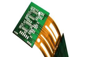
How does technology influence PCB fabrication assembly?
The emergence of 3D printing and rapid prototyping technologies has also had a significant impact on pcb fabrication assembly. These technologies allow designers to quickly create prototypes of PCBs, test their functionality, and make design changes in real-time. This not only speeds up the prototyping process but also helps identify design flaws before moving to full-scale production. Additive manufacturing techniques, such as 3D printing, have enabled the creation of more complex and customized PCB designs that were previously difficult or expensive to produce using traditional methods. As a result, engineers can now experiment with different designs and materials, resulting in faster development cycles and more innovative electronic devices.
Furthermore, advanced inspection and testing technologies have played a crucial role in improving the quality of PCB fabrication assembly. Technologies such as Automated Optical Inspection (AOI) and X-ray inspection systems allow for high-resolution monitoring of the assembly process. AOI systems use cameras and advanced image processing algorithms to detect defects such as misaligned components, soldering issues, or missing parts during the assembly process. X-ray inspection is particularly useful for checking internal connections, such as those in multi-layer PCBs or components with fine-pitch leads, ensuring that all connections are intact. These inspection technologies significantly reduce the chances of defective products reaching the market, improving the overall reliability and performance of the PCBs.
In addition to manufacturing and assembly processes, technology has also influenced materials used in PCB fabrication assembly. New materials, such as flexible substrates and high-frequency laminates, have allowed for the development of more versatile and durable PCBs. Flexible PCBs, for example, enable the design of lightweight, compact, and foldable electronic devices. These materials allow for more compact designs and open up new possibilities in areas such as wearable electronics, medical devices, and consumer gadgets. Innovations in lead-free soldering and environmentally friendly materials have also played a role in meeting regulatory requirements and reducing the environmental impact of PCB production.
Another technological factor influencing PCB fabrication assembly is the advancement in multi-layer PCB technology. As electronics become more complex, multi-layer PCBs have become essential for accommodating a higher density of components and circuitry. Multi-layer PCBs require precise alignment and advanced manufacturing techniques to ensure that each layer is correctly bonded, and connections between layers are properly made. Technologies such as laser drilling, precision etching, and advanced lamination processes have made the production of multi-layer PCBs faster, more reliable, and cost-effective.
In conclusion, technology plays a fundamental role in influencing PCB fabrication assembly by enhancing design, manufacturing, testing, and material handling. Automation, advanced software tools, 3D printing, and cutting-edge inspection technologies have all contributed to improving the speed, accuracy, and quality of the PCB fabrication assembly process. As the electronics industry continues to evolve, the integration of new technologies will only further optimize PCB production, enabling the development of smaller, faster, and more complex devices. The continued innovation in PCB fabrication assembly is a testament to the importance of technology in driving the future of electronics manufacturing.

