
Simulation in Custom PCB Design
Printed circuit board (PCB) design workflows that skip simulation will quickly find themselves in trouble. Without simulation as a gatekeeper, even well-trained engineers risk making mistakes that will cost time and money to fix later on. With the right strategy, PCB designers can avoid these costly mistakes by leveraging simulation tools throughout the entire process.
Simulating custom PCB designs is essential to optimize a design before committing to physical prototypes. The ability to simulate hypothetical, unbuildable circuits enables exploring the true electrical potential of a schematic topology, separate from practical implementation constraints. Insights gained from these simulations guide design trade-offs required to transform the idealized schematic into a real manufacturable product. These simulations help to predict performance boundaries and provide a low-risk, cost-effective method of optimization before committing to expensive physical prototypes.
However, it’s important to understand the strengths and limitations of both simulation and prototype testing. A combination of both is essential to ensuring that your final product meets industry standards and satisfies end users. Simulation is best leveraged early in the design process to provide fast and efficient iterations, while physical prototypes are needed for comprehensive performance validation under real-world conditions.
Most simulation tools are designed with certain component models in mind. For example, most are capable of simulating simple components with known parameters like resistors, capacitors, and inductors. This type of modeling works well for linear and digital circuits, but it cannot account for the varying electrical behavior of complex analog, digital, or mixed-signal circuits. Fortunately, most of these components can be modeled using more advanced methods. This includes modeling the effects of temperature and component variations, which can significantly impact a design’s performance.
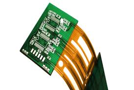
The Role of Simulation in Custom PCB Design
For most custom pcb fabrication designs, it is important to qualify the electrical behavior of a circuit before moving on to the layout stage. Performing simulations at this stage can help reduce noise and improve signal timing, especially on high-speed digital buses. Specifically, eye diagram comparisons, S-parameter simulations, and impedance calculations can be used to verify that the intended design will perform as expected in the actual PCB layout.
While these simulations can be very useful in identifying problems, it is important to remember that they do not fully reflect the true behavior of the design. Noise, signal coupling/crosstalk, radiated and conducted emissions may not be accounted for by the model. It is therefore crucial to perform targeted physical testing on a physical prototype to validate the simulation results.
A modern workflow for PCB design uses simulation as a gatekeeper at key points in the process. This helps to prevent errors and issues that would otherwise be difficult or impossible to discover during testing and prototyping. It also provides a more efficient and cost-effective approach to validation, reducing the need for time-consuming rework that can delay production and delivery of a product.
Although the initial investment in learning how to use simulation tools can be a bit intimidating, the long-term benefits are significant. By implementing simulation throughout the design process, you can minimize costly reworks and save time and money that could be spent on other critical activities like requirement specializations, schematic design, and layout.

