
role of copper plating in PCB fabrication and assembly
Copper plating plays a vital role in PCB fabrication and assembly, serving as a foundational process that significantly impacts the performance, functionality, and reliability of the final printed circuit board. During PCB fabrication, copper is used to create the conductive pathways that allow electrical signals to flow between components. The copper plating process is essential for ensuring that these pathways are properly formed and capable of carrying the electrical current without issues such as signal loss, interference, or short circuits.
In the early stages of PCB fabrication, a copper-clad laminate is used as the base material for the board. This laminate consists of a layer of copper foil bonded to a substrate, which is typically made from materials such as fiberglass or resin. Copper plating is then used to enhance the copper layers and establish the necessary conductive traces that connect the various components on the board. These copper traces are carefully designed to create the electrical connections specified in the PCB’s schematic diagram. The copper plating process allows for precise control over the thickness and quality of the copper layer, which is critical for ensuring the board meets the electrical and mechanical requirements of the final design.
One of the main roles of copper plating in pcb fabrication and assembly is to ensure the creation of reliable electrical connections between the various pads, traces, and vias on the board. Vias, which are small holes that allow electrical connections between different layers of the PCB, are especially important in multi-layer PCBs. Copper plating is used to coat the inner walls of these vias, creating conductive paths that connect different layers of the board. Without copper plating in the vias, the board would not be able to support multi-layer designs, which are crucial for more complex PCBs that require higher component density or enhanced electrical performance.
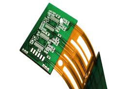
What is the role of copper plating in PCB fabrication and assembly?
Another significant role of copper plating is to provide the necessary strength and durability for the PCB’s electrical connections. The copper layers must be thick enough to withstand the heat and electrical load that the board will experience during normal operation. Copper plating ensures that the traces and vias are strong and capable of handling the stresses imposed by soldering, component mounting, and electrical operation without failing. The plating process also contributes to the board’s overall longevity, as it helps to prevent issues such as oxidation or corrosion, which could compromise the functionality of the board over time.
Additionally, copper plating is used to form the pads where components will be soldered during the assembly process. The precise placement of components requires accurate, clean, and robust solder pads. These copper-plated pads ensure that the components can be securely attached to the PCB, either by hand soldering or automated soldering techniques such as reflow or wave soldering. The copper plating process helps to create well-defined solder pads that prevent solder bridges, poor connections, or misalignment during the component placement process.
In PCB assembly, copper plating is essential for maintaining the integrity of the electrical connections as components are mounted on the board. Once the components are placed, solder paste is applied to the copper-plated pads, and the board goes through the reflow soldering process. The copper plating helps ensure that the solder bonds well to the pads and creates strong electrical connections that are essential for the board’s proper functionality. Without proper copper plating, the solder joints may be weak, resulting in unreliable or malfunctioning connections.
Finally, copper plating plays an important role in heat dissipation. As electronic components operate, they generate heat, and the PCB must be designed to dissipate that heat to prevent damage to the components or the board itself. The copper plating helps spread heat across the board and assists in the thermal management of high-power components, ensuring that the PCB can function reliably under varying temperatures.
In conclusion, copper plating is a crucial process in PCB fabrication and assembly, directly influencing the electrical performance, strength, and durability of the final PCB. From forming conductive traces and vias to ensuring reliable component placement and heat dissipation, copper plating ensures that the PCB functions as intended. Its role in creating robust electrical connections and supporting the assembly process makes it indispensable in the production of high-quality, reliable printed circuit boards used in a wide range of electronic devices.

